Page 1 of 1
My GEM VMU
Posted: Sun Mar 10, 2019 3:55 pm
by originalself
Took awhile to finish due to lack of time but the hardware part is done. I completed assembly of my GEM and I like the board.
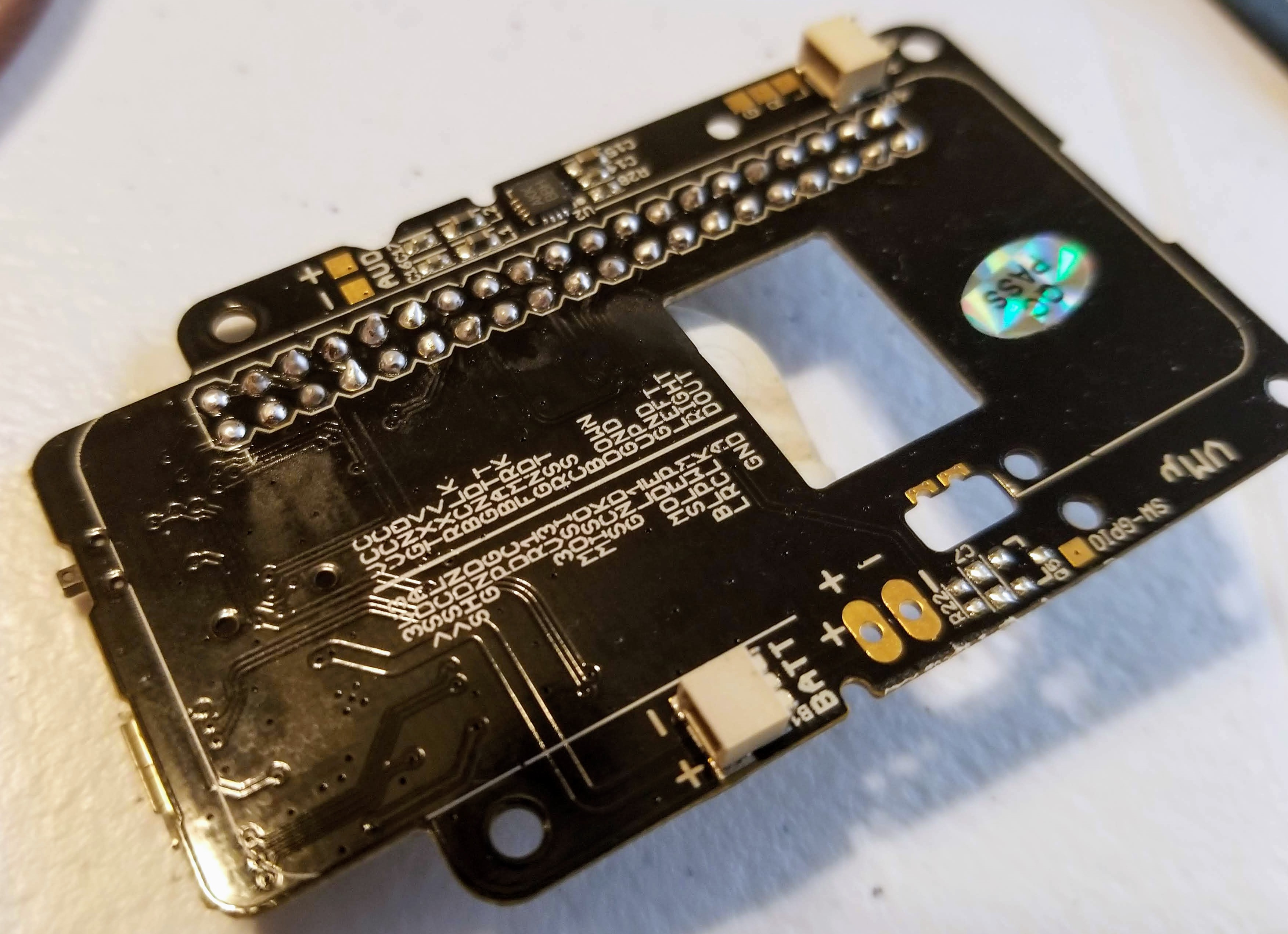
Board tinned.
- 20190302_084328.jpg (963.86 KiB) Viewed 11677 times
Case prepped. The plastic was softer than I expected. Flush cutters did the whole job. I did end up needing to trim the side walls on the back piece as well later.

- 20190302_091718.jpg (1.08 MiB) Viewed 11677 times
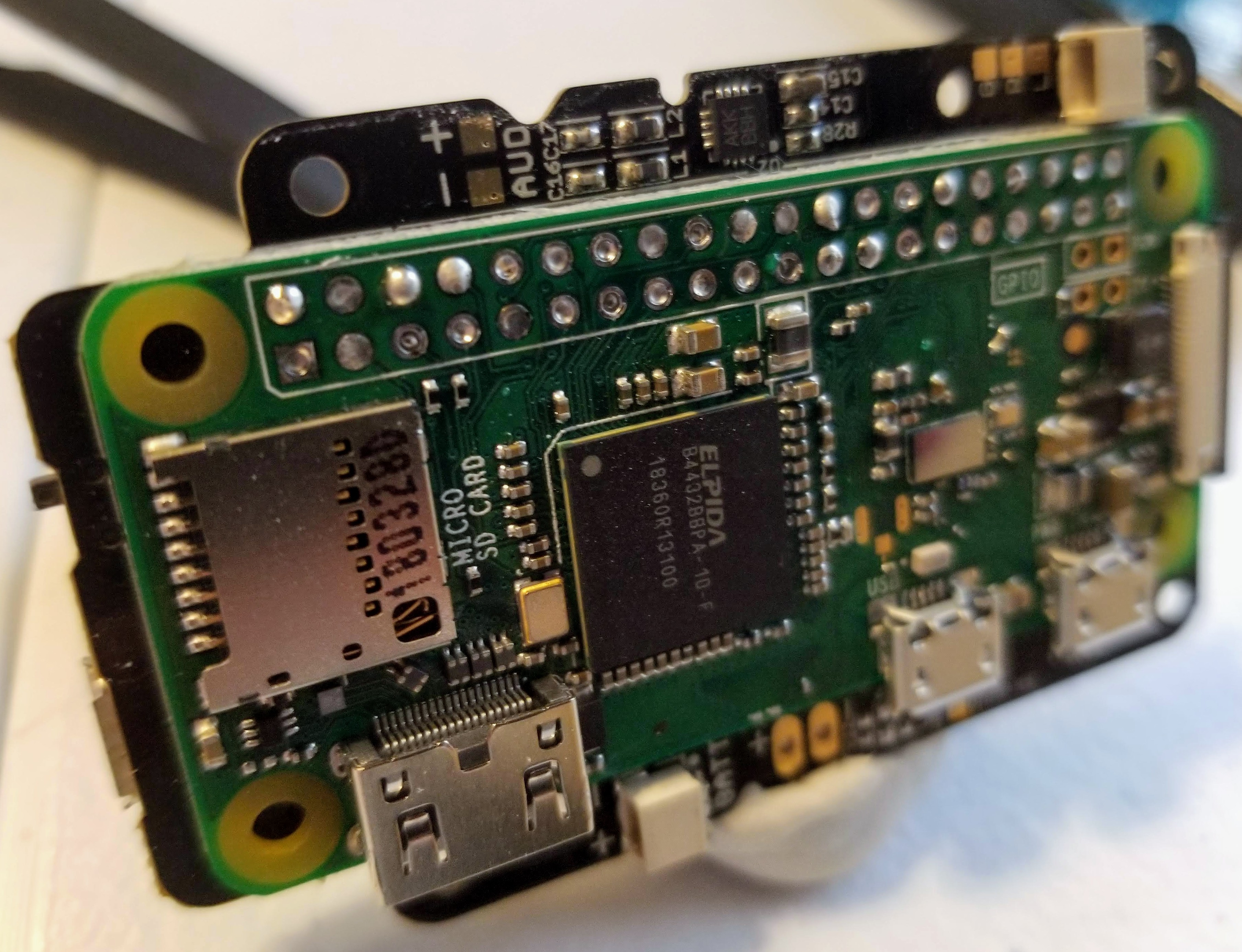
First batch of soldering done. Thank goodness for all the test pads on the back. Out of 40 pins I had to redo 8.
- 20190302_090611.jpg (1.69 MiB) Viewed 11677 times
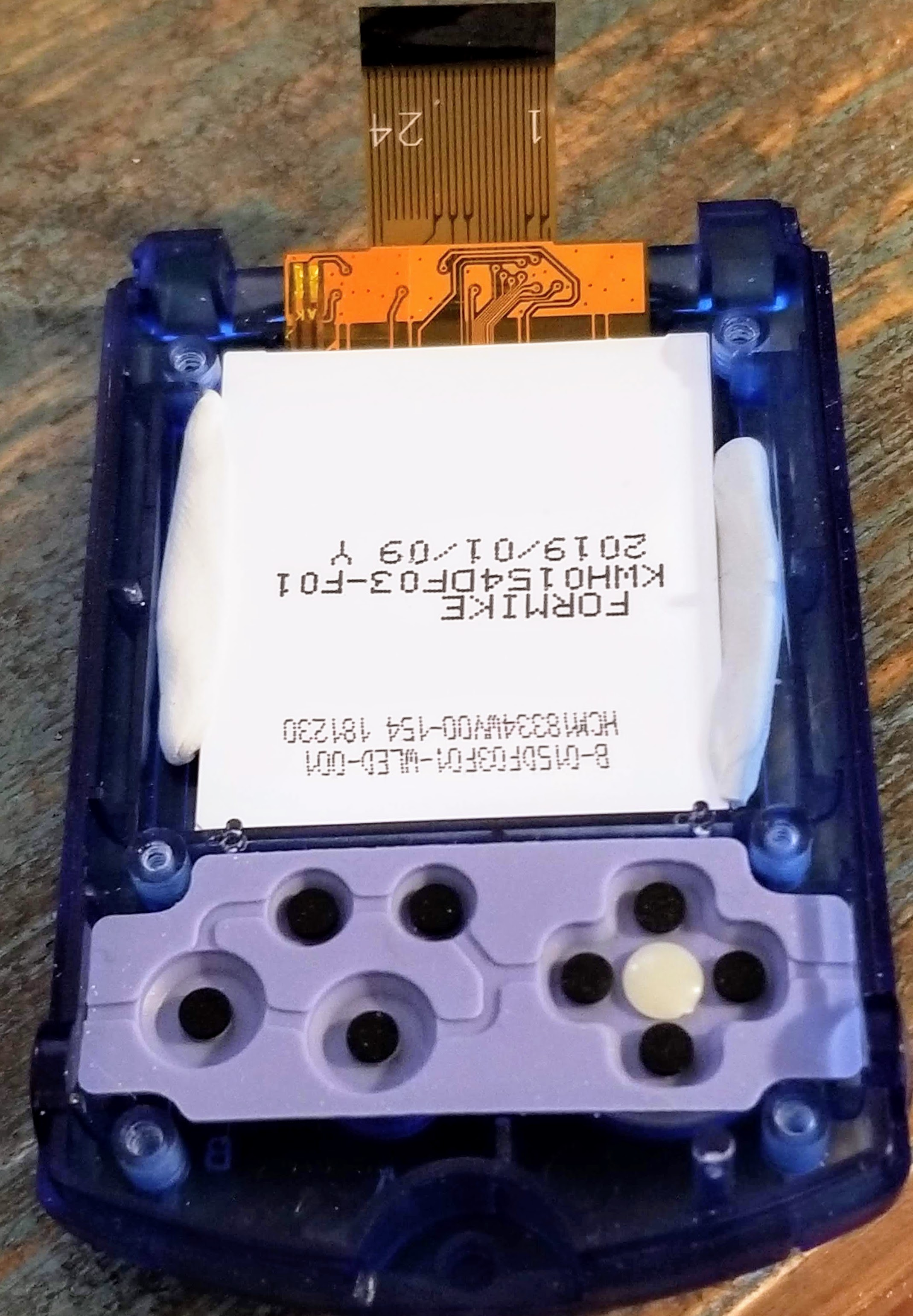
Screen in.
- 20190310_141237.jpg (716.38 KiB) Viewed 11677 times
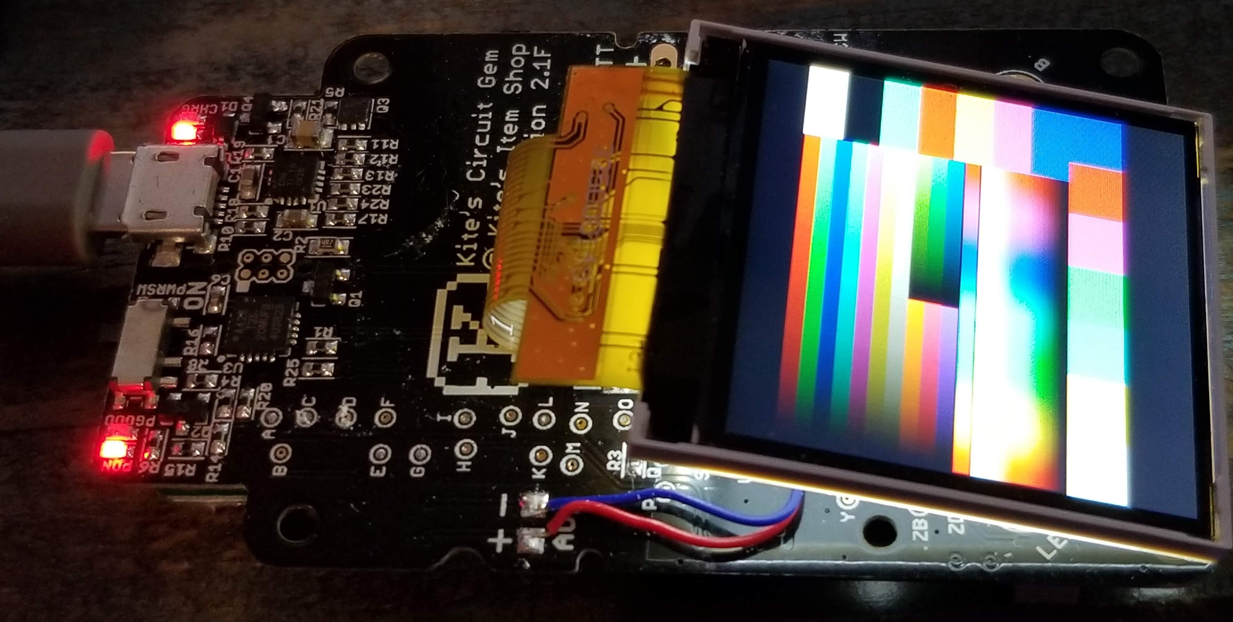
Test boot.
- 20190310_135721.jpg (870.29 KiB) Viewed 11677 times
All closed. Tight fit but I removed nothing from the zerow. I used a small 350 battery.
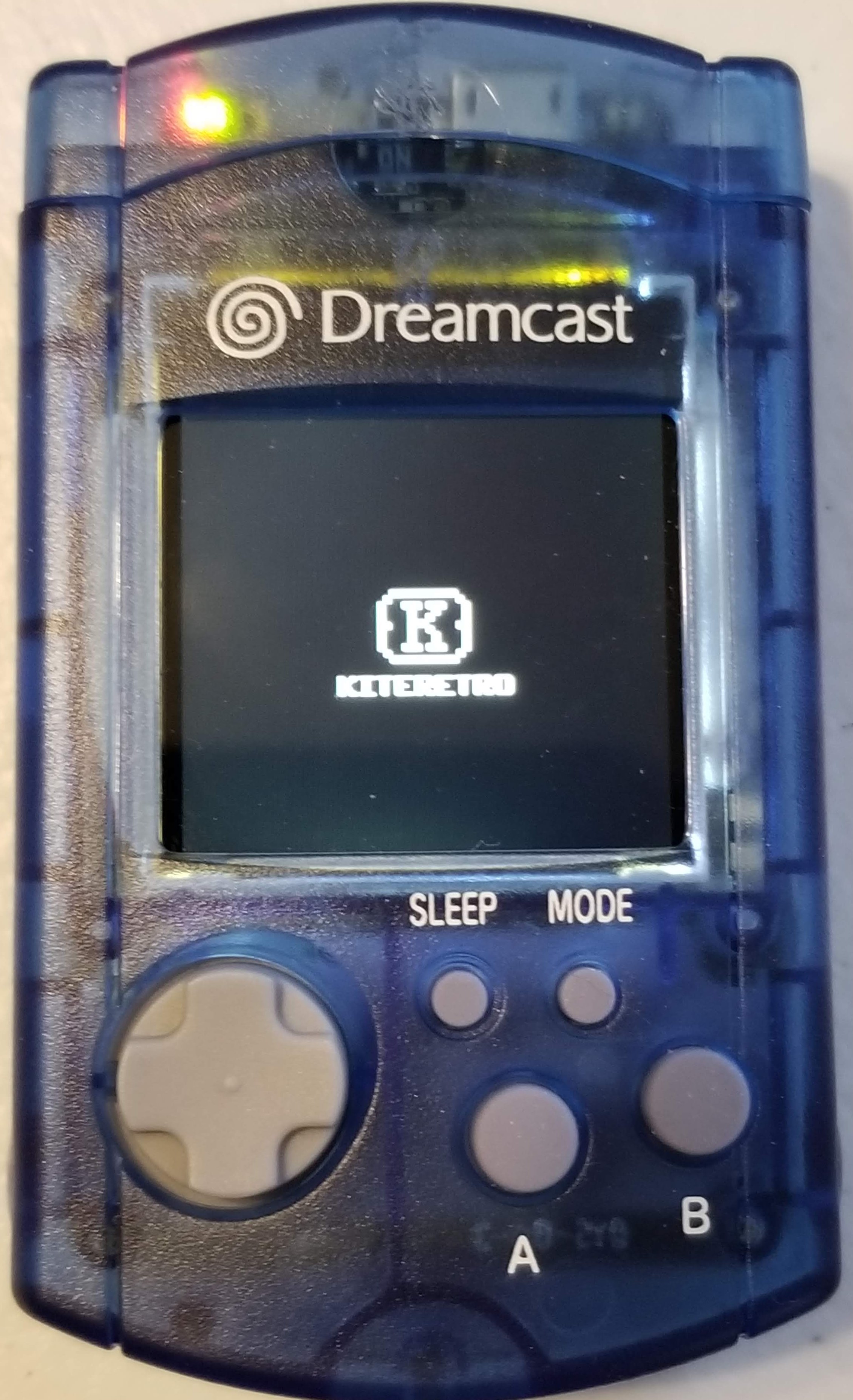
- 20190310_142943.jpg (1023.87 KiB) Viewed 11677 times
Edit:
Software was very easy to setup. Writing all the WiFi info in ahead of time like the wiki suggested meant I never even needed to plug in a keyboard. I am damn impressed with the pre configured image. This was a fun project.
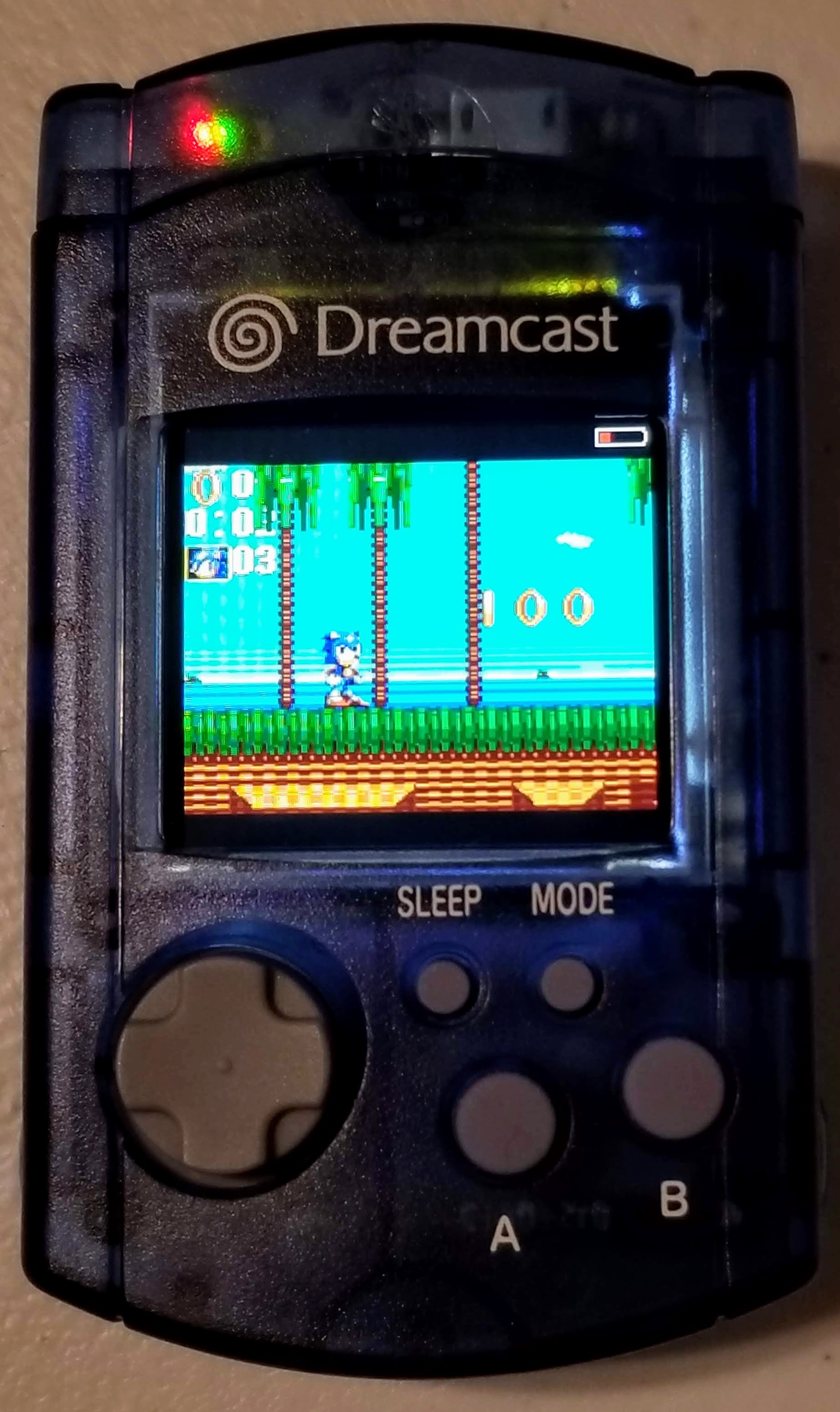
- 20190310_203613.jpg (601.98 KiB) Viewed 11658 times
Re: My GEM VMU
Posted: Mon Mar 11, 2019 10:57 am
by Robochris
Nice work. Did you remove the usb and hdmi ports?
Re: My GEM VMU
Posted: Mon Mar 11, 2019 11:07 am
by sygyzy
Great clean build!
Silly question but I couldn't figure out where the test pads for about a dozen points were. I have seen the diagram but for example, for LCD DC, it's point J but uh where is the partner pad? I don't see it anywhere on the PCB. Same with the other LCD, also BATT MON, TXD, RXD, etc. Any help would be appreciated.
Re: My GEM VMU
Posted: Tue Mar 12, 2019 12:17 am
by originalself
Robochris wrote: ↑Mon Mar 11, 2019 10:57 am
Nice work. Did you remove the usb and hdmi ports?
Nope. I removed nothing.
Re: My GEM VMU
Posted: Tue Mar 12, 2019 12:22 am
by originalself
sygyzy wrote: ↑Mon Mar 11, 2019 11:07 am
Great clean build!
Silly question but I couldn't figure out where the test pads for about a dozen points were. I have seen the diagram but for example, for LCD DC, it's point J but uh where is the partner pad? I don't see it anywhere on the PCB. Same with the other LCD, also BATT MON, TXD, RXD, etc. Any help would be appreciated.
J is pin 13 on the pi header.
https://github.com/kiteretro/Circuit-Ge ... it-Gem-FAQ So you touch the test pads and pins on the corresponding header on the other side. It’s rather awkward but invaluable.
Re: My GEM VMU
Posted: Tue Mar 12, 2019 2:49 am
by sygyzy
Hi, I understand that J = 13 but where is LCD DC?
Re: My GEM VMU
Posted: Tue Mar 12, 2019 4:38 am
by kite
sygyzy wrote: ↑Tue Mar 12, 2019 2:49 am
Hi, I understand that J = 13 but where is LCD DC?
They are alphabetical ordered vertically, so follow the test points down. J is to the bottom left of the [K] logo on the front, under 'I' and above 'L'
Re: My GEM VMU
Posted: Sat Feb 08, 2020 9:48 pm
by Spyder
UltraPunch wrote: ↑Sat Feb 08, 2020 6:22 pm
This is probably a dumb question, however; What is the point of WiFi for these?
SSH games in, download game art, software updates, etc.
Re: My GEM VMU
Posted: Mon Feb 10, 2020 10:06 am
by Spyder
If you plan on setting it and forgetting it, there isn't much of a need once its all loaded. But for $5 more, I'd still go wifi. Like you said, I'd rather have it and not need it than need it and not have it.